

Building on last week’s discussion of the 5 Key Indicators for Edge AI and Humanoid Robot Development Bandwidth, Latency, Economics, Reliability, and Privacy—I want to delve deeper into Bandwidth and Latency, two critical factors intricately tied to chip packaging density and architecture.
Two Paradigms in Computer Design In computer design, we encounter two distinct architectural paradigms:
- UMA (Unified Memory Architecture): Systems without discrete GPU chips integrated directly into the motherboard.
- Discrete GPU Design: Systems with an additional GPU chip on the motherboard, in addition to the internal GPU within the CPU.
These architectures significantly influence thermal design. UMA and Discrete systems heat sources creating unique challenges for managing thermal density.
The Shift Toward Advanced Chip Packaging
With the advent of 2.5D and 3D chip packaging(TSMC CoWos, Intel foveros) high-performance components—CPUs, GPUs, and even LPDDR RAM (like Intel’s LNL design)—are now integrated into a single chip package. These innovations enhance bandwidth and latency, delivering unprecedented performance breakthroughs.However, progress comes with challenges. Intel’s Lunar Lake (LNL) architecture, despite its innovation, struggles to scale for the next generation.
This raises critical issues:
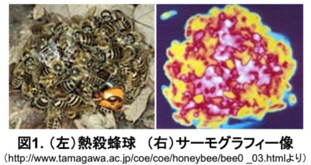
- Thermal Density Challenges Compact packaging leads to concentrated heat sources, akin to a tightly packed beehive in winter. While the core stays warm, dissipating heat becomes a significant challenge. Convection, radiation, and conduction—key mechanisms for heat transfer—are hindered by reduced surface area in dense designs.2. Issue density-Debug Complexity Integrating diverse components within a single package exponentially increases debugging difficulty. Time and resource requirements surge as diagnosing issues within such tightly packed systems becomes more intricate.
- Risk Concentration density With so much integrated into a single package, failure of any one component impacts the entire system. This centralization elevates the cost of failure far beyond that of traditional architectures.
A Bold Vision: Spherical Chip Design for thermal density issue
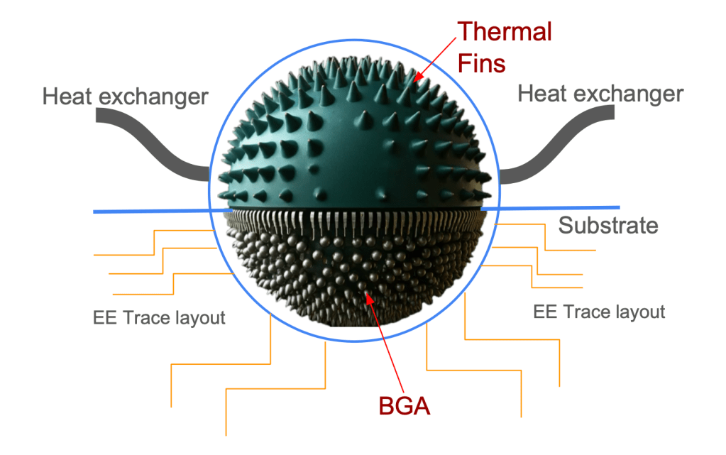
To address the thermal density challenge while enhancing bandwidth and latency, I propose an unconventional concept: spherical chip design. While this may sound futuristic, the potential advantages are compelling. A sphere is a geometric marvel, offering the smallest surface area for a given volume. Its unique properties could revolutionize chip design by:
- Maximizing capacity while minimizing external surface area.
- Enhancing thermal radiation efficiency, as heat dissipates evenly in all directions.
- Optimizing space utilization, reducing wasted structural areas.
In practice, spherical chip designs could enable more components to fit within a compact form factor while maintaining superior heat dissipation.Nature is filled with spherical structures designed for maximum efficiency—from soap bubbles to planets. Could this principle inspire breakthroughs in chip architecture, helping us navigate the trade-offs inherent in dense packaging?
While unconventional, spherical chip design challenges us to think beyond traditional approaches. For me, one of the greatest values of design thinking lies in setting clear starting points and visionary goals based on professional design and engineering experience. This is precisely why I proposed this bold and innovative idea. invites bold innovation to solve some of the toughest issues in humanoid robot development.
創新者的困境:在人形機器人開發中的帶寬與密度挑戰
延續上週關於邊緣 AI 和人形機器人開發的五大關鍵指標:帶寬、延遲、經濟性、可靠性、隱私性的討論,我想深入探討其中的帶寬與延遲,這兩個關鍵因素與晶片封裝密度和架構息息相關。
計算機設計中的兩大範式
在計算機設計中,我們會遇到兩種截然不同的架構範式:
- UMA(統一記憶體架構):系統中沒有獨立的 GPU 晶片,GPU 被集成在主板內部。
- 獨立 GPU 設計:系統除了內建在 CPU 內部的 GPU 外,還額外添加了 GPU 晶片。
這些架構會顯著影響熱設計。UMA 和離散系統的熱源會造成不同的挑戰,這對於熱密度管理提出了獨特的要求。
向先進晶片封裝技術的轉變
隨著 2.5D 和 3D 晶片封裝(例如 TSMC CoWoS、Intel Foveros)的出現,高效能元件(如 CPU、GPU,甚至是 LPDDR RAM,如 Intel 的 LNL 設計)現在被集成到單一的晶片封裝中。這些創新提升了帶寬和延遲,並實現了前所未有的性能突破。然而,這些進步同樣帶來了挑戰。儘管 Intel 的 Lunar Lake(LNL)架構具有創新性,但它在規模化上仍面臨著下一代發展的困難。
這引發了關鍵問題:
- 熱密度挑戰
緊湊的封裝會導致熱源集中,這就像是冬天擠滿蜜蜂的蜂巢。儘管核心保持溫暖,但熱量的散發成為了一個重大挑戰。對流、輻射和傳導—熱轉移的關鍵機制—在密集設計中由於表面積減少而受到了阻礙。 - 密度-除錯的複雜性
將多種元件集成在單一封裝中,會使除錯變得更加困難。由於在這些緊密封裝的系統中診斷問題變得更加複雜,因此時間和資源的需求也呈指數級增長。 - 風險集中性
在一個封裝內集成如此多的元件,如果其中任何一個元件發生故障,都會影響整個系統的運行。這種集中化使得故障的成本遠高於傳統架構。
為了應對熱密度挑戰,同時提升帶寬和延遲,我提出了一個非傳統的概念:球形晶片設計。雖然這聽起來可能像是未來的設計,但其潛在的優勢是非常吸引人的。球體是一種幾何奇蹟,對於給定的體積,它提供了最小的表面積。其獨特的屬性可能會徹底改變晶片設計,具體體現在:
- 最大化容量,同時最小化外部表面積。
- 提高熱輻射效率,因為熱量在所有方向上均勻散發。
- 優化空間利用,減少結構區域的浪費。
在實踐中,球形晶片設計可以讓更多的元件在緊湊的外形中安置,同時保持卓越的散熱效果。自然界中充滿了為最大效率設計的球形結構——從肥皂泡到行星,這些都能啟發我們在晶片架構方面的突破。
球形晶片設計雖然非常不傳統,但它挑戰我們跳出傳統思維方式。對我來說,設計思維的最大價值之一就是根據專業的設計和工程經驗,設定明確的起點和遠見目標。正因為如此,我提出了這個大膽且創新的想法,邀請我們進行大膽的創新,解決人形機器人發展中的一些最棘手的問題。
大膽的願景:球形晶片設計應對熱密度問題


發表留言